http://www.chemistrymag.org/cji/2003/056049pe.htm |
Jun. 1, 2003 Vol.5 No.6 P.49 Copyright |
Lu Shengli , Yang Mujie
(Department of Polymer Science and Engineering, Zhejiang University, Hangzhou 310027)
Received Apr.21, 2003; Supported by the National Natural Science Foundation of China (No. 20274039)
Abstract The bulk heterojunction
photovoltaic devices based on
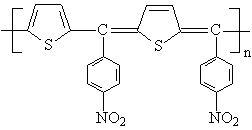
poly[(2,5-thiophenediyl)(p-nitrobenzylidene)(2,5-thiophenequinodimethanediyl)](PTNBQ) and
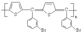
poly[(2,5-thiophenediyl)(m-bromobenzylidene)(2,5-thiophenequinodimethanediyl)](PTBBQ) as
donors , which are small-bandgap polymers, together with a soluble fullerene
derivative(PCBM) as acceptor were fabricated. Photovoltaic performance parameters were
characterized.
Keywords Small-bandgap polymer, polymer photovoltaic devices, fullerene derivative
(PCBM).
1 INTRODUCTION
Solar light is the most important source
of regenerative energy and represents mankind's only inexhaustible energy source. In the
last couple of years, the development of solar cells based on organic molecules[1]
and conjugated polymers[2-4] has progressed rapidly. Semiconducting polymers in
combination with electron accepting fullerenes were found to show an ultrafast
photoinduced charge transfer reaction[5-6] at the donor-acceptor interface,
which results in a metastable charge-separated state. Energy conversion efficiency
exceeding 3.3% under AM1.5 illumination has recently been reported[7] for bulk
heterojunction polymer photovoltaic devices. One of the limiting parameters in these
polymer photovoltaic devices is the mismatch of their absorption to the terrestrial solar
spectrum. At present, substituted poly(p-phenylene vinylene)s and polythiophenes are
typically used in the construction of polymer photovoltaic devices. The optical bandgap of
these conjugated polymers (Eg=2.0-2.2eV) is not optimized with respect to the solar
emission, which has the maximum photon flux around 1.8eV. For efficient harvesting the
terrestrial solar spectrum in conjugated polymer based photovoltaic devices, small-bandgap
polymers are needed. Poly(heteroarylene methines) are known as small-bandgap conjugated
polymers[8,9], because they contain alternating aromatic and quinoid segments
in the main chain. The use of small-bandgap polymers expands the spectral region of bulk
heterojunction solar cells and is a viable route to enhance the number of photons
absorbed.

PTNBQ
PTBBQ
PCBM
Scheme 1 The chemical structures of PTNBQ, PTBBQ and PCBM
2 EXPERIMENTAL
PTNBQ and PTBBQ were synthesized by
acid-catalyzed polymerization of p-nitrobenzaldehyde and m-bromobenzaldehyde with
thiophene, respectively[8,9]. PCBM was synthesized according to Ref [10]. The
chemical structure of them are shown in Scheme 1.
Absorption spectra were obtained using HEWLETT Packard 8453
spectrophotometer.
Photovoltaic devices were fabricated using PTNBQ+PCBM(1/4,w/w) and
PTBBQ+PCBM(1/4,w/w) as the active layer, respectively, which was spin-coated from a
toluene solution. The thickness of the active layer of PTNBQ+PCBM was 50nm and PTBBQ+PCBM
was 85nm, respectively, as determined by the Surface profilometer(Tencor Alpha-500).
Indium tin oxide (ITO) was used as the anode and 100nm thick poly(ethylene
dioxythiophene)-poly(styrene sulfonic acid)(PEDOT-PSS) layer(Bayer Batron-P) was
incorporated between ITO and the active layer to reduce device leakage. The PEDOT-PSS
layer was dried in a vacuum oven at 80ºC for 1h. Ba(barium) metal was thermally evaporated onto the top of
the active layer, finally, 170nm thick Al(aluminum) was thermally evaporated onto the top
of Ba. The deposition rates and the thickness of the evaporation layers were monitored by
a thick/rate meter(Sycon, STM100). The deposition rates were usually 0.5-1nm/s. The
cathode area defined the size of the active area was 0.15cm2. Except for
spin-casting PEDOT-PSS layer, all the fabrication steps were carried out in a nitrogen
glove box. Dark and photo I-V characteristics of the devices were measured with a Keithley
236 source-measure unit. Photo current was measured under illumination (78.2mW/cm2,AM1.5)
with a tungsten lamp. The photosensitivity was measured with a commercial photomodulation
spectroscope setup(Merlin digital lock-in, Oriel) including a xenon lamp, an optical
chopper, a monochromator and lock-in amplifier operated by PC computer. Calibrated Si
photodiode was used as the standard in the determination of photosensitivity.
3 RESULTS AND DISCUSSION
Poly(heteroarylene methines) are known as
small-bandgap conjugated polymers, because they contain alternating aromatic and quinoid
segments in the main chain[8,9,11]. From Figure 1 and Figure 2, it is
seen that both PTNBQ and PTBBQ have the broad absorption in the visible region from 400 to
600nm. The corresponding absorption edges of the spectra are at 690 and 660nm, hence the
optical bandgaps are 1.79 and 1.88eV, respectively.
Figure 1 and Figure 2 also show the absorption of PCBM, the composite
of PTNBQ with PCBM and the composite of PTBBQ with PCBM, respectively. The absorption
spectrum of PCBM is similar to that of C60, with the absorption peak at 343nm
and smaller peaks located at 420-500nm and 550-720nm, respectively. The absorption peaks
at 336nm of the composite of PTNBQ+PCBM and 337nm of the composite of PTBBQ+PCBM are
assigned to PCBM absorption, the other absorption of PCBM in visible region is almost
overlapped with those of the PTNBQ or PTBBQ. So we can deduce that the absorption of the
composite is just superposition of the peaks of them and PCBM without any indications of
extra spectral features. This result confirms that there is no significant interaction
between the two materials in the ground state.
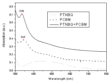
Figure 1 The UV-Vis spectra of PTNBQ
(in THF), PCBM (in toluene) and PTNBQ+PCBM (1/4,w/w) composite (in toluene)

Figure 2 The UV-Vis spectra of PTBBQ (in THF), PCBM (in toluene) and PTBBQ+PCBM (1/4,w/w) composite (in toluene)
Figure 3 and Figure 4 show
the typical I-V characteristics (both in the dark and under illumination of 78.2mW/cm2,
AM1.5) of the PTNBQ+PCBM(1/4,w/w) and PTBBQ+PCBM(1/4, w/w) devices. Their device
characteristics under AM1.5 are listed in Table 1.
The low rectification of the PTNBQ+PCBM device (87.3 at ±2V) reflects
the rather poor film-forming properties of PTNBQ, which are induced by the low molecular
weight( ![]() )[8]. During the device
fabrication, the thickness of PTNBQ+PCBM is only 50nm, it could not be increased anymore,
consisting with the low molecular weight of PTNBQ. On the contrary the thickness of
PTBBQ+PCBM composite can be reached 85nm. This not only manifest the molecular weight of
PTBBQ is larger than that of PTNBQ, but also it can absorb more photons resulting higher
energy conversion efficiency.
)[8]. During the device
fabrication, the thickness of PTNBQ+PCBM is only 50nm, it could not be increased anymore,
consisting with the low molecular weight of PTNBQ. On the contrary the thickness of
PTBBQ+PCBM composite can be reached 85nm. This not only manifest the molecular weight of
PTBBQ is larger than that of PTNBQ, but also it can absorb more photons resulting higher
energy conversion efficiency.
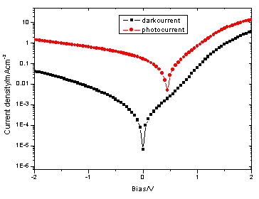
Figure 3 I-V characteristics of device
ITO/PEDOT-PSS/PTNBQ+PCBM (1/4,w/w)/Ba/Al
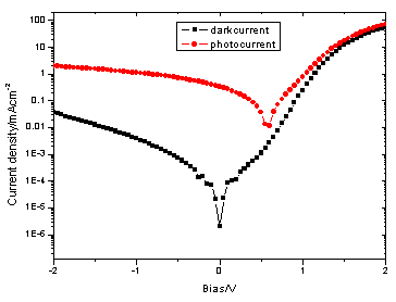
Figure 4 I-V characteristics of device ITO/PEDOT-PSS/PTBBQ+PCBM (1/4,w/w)/Ba/Al
Table 1 Photovoltaic performance parameter of the devices under AM1.5
Active layer |
Isca |
Vocb |
FFc |
hed |
Re |
PSf |
IPCEg |
PTNBQ+PCBM |
0.169 |
0.45 |
23.61 |
0.023 |
87.3 |
0.0057 |
1.45 |
PTBBQ+PCBM |
0.339 |
0.60 |
21.12 |
0.055 |
1501 |
0.017 |
4.4 |
a
short circuit current density. b open circuit voltage. c fill factor. d energy conversion efficiency. e rectification. f photosensitivity. g incident photo-current conversion efficiency. Compared
Figure 5 with Figure 1 and Figure 2, the photosensitivity form of these two devices are
almost identical and coincide quite well with their absorption spectra. The
photosensitivity peak at about 330nm in Figure 5 comes from the absorption by PCBM, while
the broadened peaks at 400-500nm originate from combination of PCBM and PTNBQ or PTBBQ. A
small shoulder in the ranger 600-800nm comes from PCBM absorption. The photosensitivity
and incident photo-current conversion efficiency of PTBBQ+PCBM device is larger than that
of PTNBQ+PCBM in the whole spectral region probably due to the reason discussed above. The
photosensitivity and IPCE data are also summarized in Table 1.

Figure 5 Photosensitivity of
photovoltaic devices with PTNBQ+PCBM(1/4,w/w) and PTBBQ+PCBM(1/4,w/w) at zero bias
4 CONCLUSION
Polymer photovoltaic devices using the small-bandgap polymers combined
with PCBM as the active layer were fabricated. They show photovoltaic effect. In the
future, synthesizing new small-bandgap conjugated polymers with high molecular weight
maybe the way to obtain high energy conversion efficiency of photovoltaic devices.
REFERENCES
[1] Wöhrle D, Meissner D. Adv. Mater., 1991, 3 (3): 129.
[2] Yu G, Gao J, Hummelen J C et al. Science, 1995, 270: 1789.
[3] Shaheen S E, Brabec C J, Sariciftci N S. Appl. Phys. Lett., 2001, 78 (6): 841.
[4] Roman L S, Andersson M R, Yohannes T et al. Adv. Mater., 1997, 9 (15): 1164.
[5] Sariciftci N S, Smilowitz L, Heeger A J et al. Science, 1992, 258: 1474.
[6] Morita S, Zakhidov A A, Yoshino K et al. Solid. State Commun., 1992, 82: 249.
[7] Brabec C J, Shaheen S E, Winder C et al. Appl. Phys. Lett., 2002, 80 (7): 1288.
[8] Chen W C, Jenekhe S A. Macromolecules, 1995, 28: 454.
[9] Chen W C, Jenekhe S A. Macromolecules, 1995, 28: 465.
[10] Hummelen J C, Knight B W, Lepec F et al. J. Org. Chem., 1995, 60: 532.
[11] Van Mullekom H A M, Vekemans J A J M, Havinga E E et al. Mater. Sci. Eng., 2001, 32:
1.