http://www.chemistrymag.org/cji/2006/086039ne.htm |
Jun. 1, 2006 Vol.8 No.6 P.39 Copyright |
Sun Weili 1, Li Yongxiu1,
Liu Huibiao2, Li Yuliang2,
Gan Haiyang2, Jiu Tonggang2, Li Yongjun2, He
Xiaorong2, Wang Ning2, Jiang Lei2
(1Depatrment of Chemistry, Nanchang University, Nanchang 330049; 2CAS
Key Laboratory of organic solid, Centre for Molecular Sciences, Institute of Chemistry,
Chinese Academy of Sciences, Beijing 100080, China)
Abstract The oriented charge
transfer salt CuTCNQ 3D nanowires arrays were easily controlled to directly grow onto
substrates from the molecular scale to the nanoscale by organic vapor-solid phase reaction
without template and catalysts.
Keywords 3D arrays, nanowires, CuTCNQ, organic vapor-solid phase reaction.
As a well-known metallic organic charge transfer (CT) salt, TCNQ (7,7,8,8-tetracyanoquinodimethane) salts based on copper (CuTCNQ), has been studied intensively[12]. CuTCNQ have exhibited semiconducting properties as well as on/off switching characteristics and memory effects, which are applied for optical and electrical record media[13]. We have previously explored a synthetic route to produce CuTCNQ nanowires on many substrates by organic vapor-solid reaction and the field emission properties of the nanowires show itself an excellent potential candidate for field emitters[14]. The results encourage us to possibly organize the CuTCNQ nanowires into 3D nanowires arrays and grow large-scale multi-dimensional nanomaterials directly onto substrates from the molecular scale to the nanoscale by controlling the experimental conditions (such as the temperature of reaction and copper quantum et al.). Recently, we developed a simple method based on the organic vapor-solid reaction for producing new aggregate nanostructures of the complex of TCNQ molecule and copper. The method of organic vapor-solid reaction that we report here has potential as a generic means for fabricating 3D nanowires arrays for various materials, and may also offer an opportunty for further applications.
We employ a copper layer with thickness of 60 nm deposited on the surface of Si (100) as copper source. The copper layers were prepared by using known methods[15]. In a typical experiment, the furnace temperature was first increased to 85°C. Then the TCNQ powder is loaded into a ceramic boat and the Si (100) substrate with a copper layer is placed on the top of the ceramic boat, which is placed at the center of a quartz tube. After the quartz tube was inserted into a horizontal tube furnace, the furnace temperature is rapidly increased to 150°C and then kept at that temperature for 1 h. Finally, the temperature was allowed to descend to room temperature. In the process, the argon gas flowing rate was kept at 60 standard cubic centimeters per minute. During the evaporation, the TCNQ vapor reacts with copper of the surface substrate. After the reaction, the Si (100) substrate was coated with a layer blue-black film, that is, constructing of CuTCNQ nanowires. The full characterization data of the products indicate the typical characteristics of CuTCNQ (See supporting information).
As expected, well-aligned CuTCNQ nanowires 3D arrays are grown on the surface Si(100) and arranged in very uniform arrays (Fig. 1). Fig. 1A shows a general view of the as-prepared CuTCNQ 3D nanowires arrays on the surface of Si(100). Fig. 1B shows the SEM images with higher magnifications. It is interested in that those nanowires formed pyramid-like bundles by the top of nanowires adhering to each other, and a new nanowire grew form the top of pyramid-like bundle, which seemed an antenna on the top of pyramid. Those bundles aligned to oriented 3D pyramid with antenna arrays on the surface of Si(100). From the typical area of CuTCNQ 3D nanowires arrays (Fig. 1C), those nanowires exhibited a uniform diameter of about 40 nm. The top of bundles consisted of a block of CuTCNQ, and the nanowires formed bundles by the block conglutinated with one another, also the antenna-like nanowires grew from the block with a uniform diameter and length of about 40 nm and 700nm, respectively (Fig. 1D). The results of energy-depressive spectrum (EDS) shows that the CuTCNQ nanowires are composed of copper, carbon and nitrogen elements (Fig. 2). The products were also characterized by FT-IR spectra, which provide evidence for bonding Cu and TCNQ. CuTCNQ nanowires exhibit a strong, broad n (C≡N) absorption band at 2202 cm-1. Compared with the spectrum of pure TCNQ molecule, the spectrum of CuTCNQ complex shows an obvious change. The absorption at 825 cm-1 is consistent with the presence of TCNQ- and not TCNQ, TCNQ2- or mixed-valence stacks of TCNQ- and TCNQ, [14] that is very sensitive to changes in oxidation state. The absorption of CN group at 2202 cm-1 indicates that the CuTCNQ nanowires is phase I of CuTCNQ.[14]
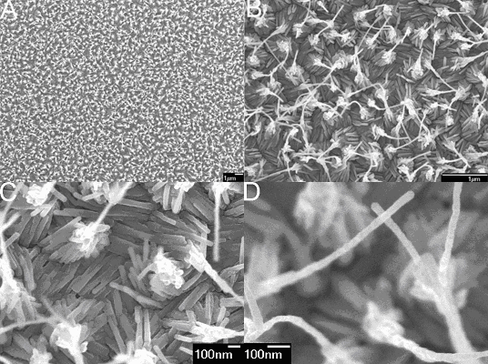
Fig. 1 SEM images of CuTCNQ 3D nanowires arrays as-grown on the surface of Si(100). (A) A general view of the sample. (B) A high magnification SEM image. (C) A typical area of CuTCNQ 3D nanowires arrays. (D) A single CuTCNQ nanowires on the top of bundle nanowires.
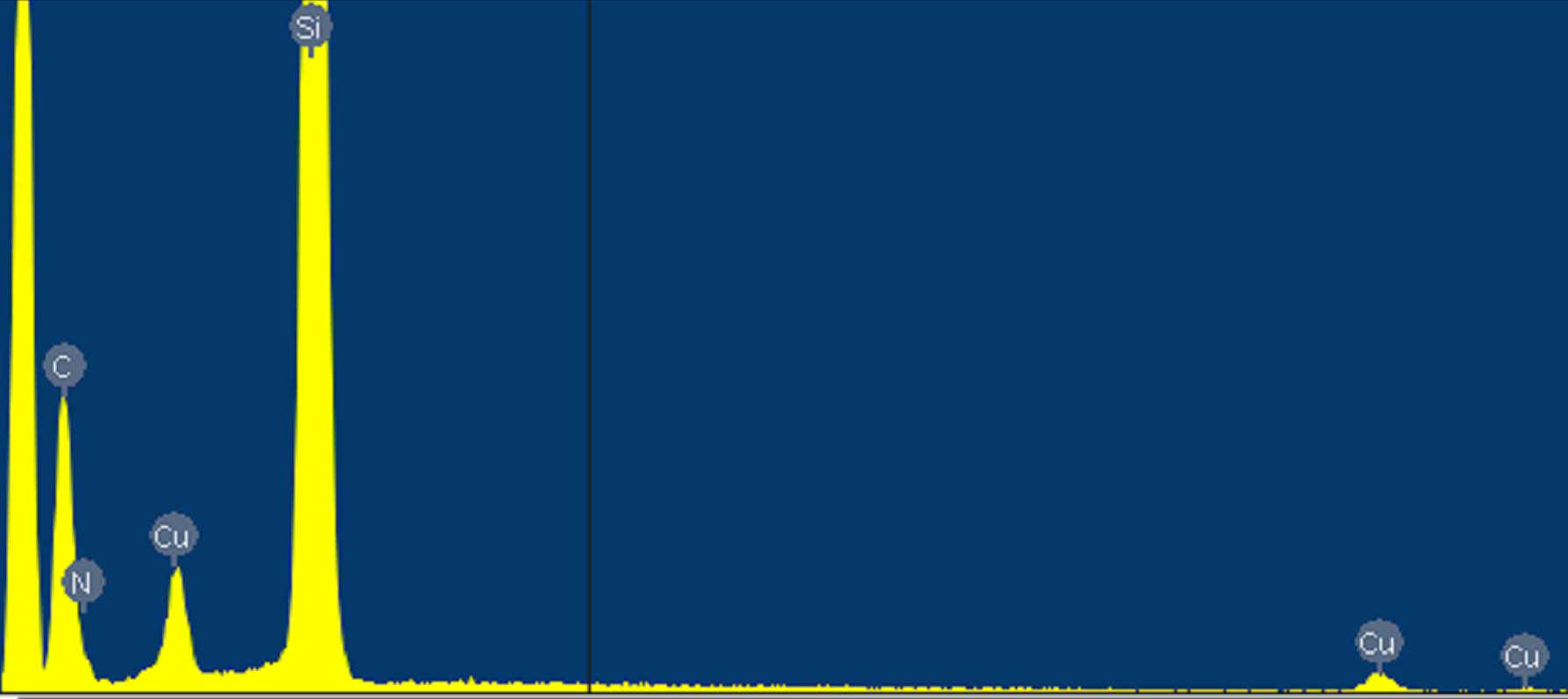
Fig. 2 Energy-depressive spectrum of CuTCNQ 3D nanowires arrays.
The growth of CuTCNQ 3D nanowires arrays can be explained on the basis of initial nucleation and nuclei movement on the surface of Si (100). In the synthesis process, the TCNQ powders are rapidly heated to 85°C to vaporize and react with copper atoms on the Si(100) surface where organic vapor solid reaction occurred to form CuTCNQ complexes. The initial CuTCNQ aggregates nanocluster on the Si(100) surface, which is used as the nucleation centers determining the growth of CuTCNQ nanowires, and the CuTCNQ nanorods grow from the nucleation sites. The nanorods gradually grow for yielding nanowires with increasing reaction time. With the reaction temperature rapidly increasing, the quantum of TCNQ vapor increased, the rate of producing TCNQ vapor is higher than the rate of reacted TCNQ vapor with copper. These TCNQ vapors that did not participate in reaction with Cu agglomerated small liquid droplets on the top formed CuTCNQ nanowires arrays. These small TCNQ liquid droplets on the top are able to composite large droplets because of high density of CuTCNQ nanowires and the short distance among those nanowires, these droplets can further induce on the top to form bundles of CuTCNQ nanowires. Finally the large liquid droplets were acted as nucleation center to grow new nanowires arrays until the copper on the surface of Si(100)were consumed completely and the CuTCNQ 3D nanowires arryas were successfully fabricated. The dimensional arrays of the TCNQ nanowires are also found to strongly depend on reaction temperature. Under the same condition, the furnace temperature increases to 150°C from room temperature, the CuTCNQ 1D nanowires arrays were formed on the surface of Si(100) (Figure 3). The SEM images show that the diameters of uniform nanowires are about 55 nm (Figure 3B). The results show that the different dimensional arrays formed may be due to the rate of TCNQ vapor yielded from starting temperature of 25°C is slower than that of TCNQ vapor yielded at a furnace temperature from 85°C to 150°
C.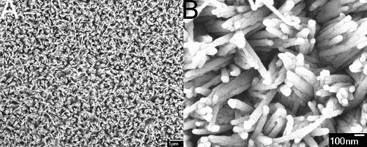
Fig. 3 (A) Low magnification SEM image of CuTCNQ 1D nanowires arrays. (B) High magnification SEM image of CuTCNQ nanowires. In summary, oriented charge transfer salt CuTCNQ 3D nanowires arrays were easily controlled to synthesize by organic vapor-solid phase reaction without template and catalysts. This approach would be led to the development of a novel general concept-purpose-built materials, which is dedicated to design of functional materials with the appropriate controlling orientation and dimension in order to probe, tune, and optimize their physical properties. Considering the unique properties of CuTCNQ complex, its 3D nanowires arrays should be of importance for both theoretical investigations and practical applications. Acknowledgments The authors would like to thank Prof. Lifeng Chi and Dr. Xiaochun Wu for offering the substrates with copper layer. REFERENCES
1. Y. Cui, Q. Wei, H. Park, C. M. Lieber, Sicence, 2001, 293, 1289.
2. Y. Xia, P. Yang, Y. Sun, Y. Wu, B. Mayers, B. Gates, Y. Yin, F. Kim, Y. Yan, Adv. Mater., 2003, 15, 353.
3. M. S. Arnold, P. Avouris, Z. W. Pan, Z. L. Wang, J. Phys. Chem. B., 2003, 107, 659.
4. K. S. Stoyan, J. M. B. Kyle, J. C. Christppher, A. G. Bartosz, Adv. Mater., 2005, 17, 751.
5. J. Johnson, H. Yan, P. Yang, R. Saykally, J. Phys. Chem. B, 2003, 107, 8816.
6. (a) A. P. Alivisatos, Science, 1996, 271, 933. (b) U. Banin, Y. W. Cao, D. Katz, O. Millo, Nature, 1999, 400, 542.
7. Z. T. Zhang, Z. W. Pan, S. M. Mahurin, S. Dai, Chem. Commun., 2003, p.2584.
8. T. M?rtensson, P. Carlberg, M. Borgstr?m, L. Montelius, W. Seifert, L. Samuelson, Nano Lett., 2004, 4, 699.
9. R. Liu, A. Vertegel, E. W. Bohannan, T. A. Sorenson, J. A. Switzer, Chem. Mater., 2001, 13, 508.
10. M. H. Huang, S. Mao, H. Feich, H. Yan, Y. Wu, H. Kind, E. Weber, R. Russo, P. Yang, Science, 2001, 292, 1897.
11. (a)G. H. Lee, S. H. Huh, J. W. Jeong, S. H. Kim, B. J. Choi, H. C. Ri, Chem. Mater., 2003,15 , 504. (b) L. Vayssieres, K. Keis, S. E. Lindquist, A. Hagfeldt, J. Phys. Chem. B, 2001, 105, 3350. (c) M. Srinivasarao , D. Collings, A. Philips, S. Patel, Sicence, 2001, 292, 79. (d) S. Wang, C. Zeng, S. Lai, Y. J. Juang, Y. Yang, L. J. Lee, Adv. Mater., 2005, 17, 1182.
12. (a) R. Long, R. Sparks, Acta Cystrallogr. 1965, 18, 932. (b) A. K. Neufeld, I. Madsen, A. M. Bond, C. F. Hogan, Chem. Mater., 2003, 15, 3573 and references there in..
13. (a) R. Potember, T. Poehler, D. Cowan, Appl. Phys. Lett., 1979, 34, 405 (b) D. Jerome, H. J. Schulz, Adv Phys., 2002, 51, 293.
14. H. B. Liu, Q. Zhao, Y. L. Li, Y. Liu, F. S. Lu, J. P. Zhuang, S. Wang, L. Jiang, D. B. Zhu,D. P. Yu, L. F. Chi, J. Am. Chem. Soc. 2005, 127, 1120.
15. R. G. Nuzzo, L. H. Dubois, D. L. Allara, J. Am. Chem. Soc., 1990, 112, 558.
电荷转移盐三维纳米线阵列的控制合成
孙伟丽1, 李永绣1, 刘辉彪2, 李玉良2,
甘海洋2, 酒同钢2, 李勇军2,
贺晓蓉2, 王宁2,江雷2
(1南昌大学化学系,江西南昌 330049; 2中国科学院化学研究所,有机固体中科院重点实验室,
分子科学中心,北京,100080)
摘要
在无模板和催化剂的温和条件下,利用有机气固相反应在硅片基底上直接合成了有机电荷转移盐CuTCNQ纳米线阵列,并且通过调节反应条件可以控制合成CuTCNQ纳米线三维阵列。
关键词 纳米线 三维阵列 有机气固相反应 CuTCNQ