http://www.chemistrymag.org/cji/2002/04a046pe.htm |
June 30,
2002 Vol.4 No.10 P.46 Copyright |
Investigations of electrodeposition behavior of silver on p-type silicon(100) surface
Wang Chunming, Tong Hao, Li Mengke, Sun
Qiaoyu
(College of Chemistry and Chemical Engineering, Lanzhou University, Lanzhou 730000, China)
Received Feb.28, 2002
; Supported by the National Natural Science Foundation of China (20073017).Abstract The electrodeposition and the
anodic stripping behavior of silver on p-silicon (100) were studied by using cyclic
voltammetry (CV). The silicon wafer was processed to be a unique working electrode. No
underpotential deposition on the silicon substrate was observed. The electrodeposition
kinetics is controlled by an initial nucleation on active sites and then a hemispherical
diffusion of silver ions towards the growing Ag cluster. Atomic force microscopy (AFM) was
used to investigate the surface morphology of the electrodeposited silver film. As a
comparative study, the method of electroless deposition of silver on p-silicon (100) was
adopted. The experimental results indicated that the obtained silver film by
electrodeposition method can be used as a seed layer in electroless deposition of silver.
Keywords Electrodeposition, Silver, Silicon (100) wafer, Cyclic voltammetry, Atomic
force microscopy.
The technology of metal deposition on silicon
wafer has been widely applied in the manufacture of ultra-large-scale integration (ULSI)
and computer engineering [1]. Aluminum and copper[2] are the often
used metals in this case. However, with the development of the ULSI, some metals with more
excellent electronics and physics properties are desired. In comparison to other metals,
silver deserves special attention. Silver does not diffuse into silicon. It crystallizes
easilyŁ¬for which can
minimize voids in the deposited metal layer. Its lower resistivity of 1.61mW-cm versus 1.68mW-cm for Cu and 2.65mW-cm for Al allows higher current
densities and narrower lines and hence faster conducting rates[3]. Also Ag has
good via-trench filling capability and satisfactory adhesion to the silicon surface [4].
So it is expected to replace Al and Cu in the development of ULSI technology now and in
the future.
By comparison with other deposition techniques, electrodeposition of
metal offers unique possibilities for an exact and easy control of the deposition
conditions and represents a straight-forward approach for locally structuring and
modifying surface[5]. The surface structure of electrodeposited metal is
directly related to the mechanism and kinetics of metal phase formation processes.
However, there is only a few of the works[6] about electrodeposition of silver
on silicon wafer was reported up to date. So, the study of the electrodeposition behavior
of silver on silicon wafer is still a basic work for future application.
1.1 Instrumentation
A CHI-660 Electrochemical workstation (USA) was used. A 40ml of homemade Teflon cell was used in a 3-electrode configuration. The silicon wafer served as the working electrode with a disc area of 0.07069cm2 for which the wafer was mounted to a small hole of the bottom of the cell. Electrical contact was made to the backside of the wafer using an indium-gallium (mixture 3:1 by mass) eutectic paste. The counter electrode was a platinum wire, dipped directly into the supporting electrolyte. The reference electrode was a saturated Hg2Cl2/Hg (SCE) electrode with a jacketed outside salt bridge (the outside bridge was filled with saturated KNO3 solution). An ultrasonic cleaner, a pHs-4 acidic meter and a P47-SPM-MDT atomic force microscopy (Solver) with tapping mode were used.
1.2 Chemicals and materials ˇˇ ˇˇˇˇˇˇˇˇˇˇˇˇˇˇˇˇˇˇˇˇˇˇˇˇˇˇˇˇˇˇˇˇ
0.1000M AgNO3 stock solution was prepared by dissolving 4.2470g AgNO3 in 250ml water in a brown flask. A solution of 2.0M NH3 was prepared by diluting 35.8ml concentrated NH4OH (61%) with water to 250ml. HCl (36%), H2O2Ł¨31%Ł©, NH4F and HF(40%) were used. Chemicals used were all of analytical-reagent grade coming from Shanghai without further purification. The double-distilled water was used throughout. Nitrogen was used for removing the dissolved oxygen in solution. A Ł¨100Ł©p-type silicon wafer with resistivity of 15~20Wcm and a thickness of 650ˇŔ25mm(Beijing Youyan silicon villa semiconductor company) was used.
1.3 Wafer treatment
The silicon wafer was cut to produce square samples with the 1cm2 surface area. Firstly the wafer was cleaned in the ultrasonic cleaner in water for 10min. Then the wafer was immersed into a hot(80ºC) solution of H2O2:NH4OH:H2O (1:1:5) for 5min and next into another hot(80ºC) solution of H2O2:HCl:H2O (1:1:6) for 5min to remove possible contamination. Lastly the wafer was treated in a solution of HF:NH4F:H2O (1:1:5) for 2min at room temperature to remove silicon native oxide. The wafer was rinsed with water after each cleaning step. After finishing all treatment procedure as above, the wafer was immediately preserved in a vacuum dryer so as to avoid the oxidation and ready for the electrodeposition use.
1.4 CV procedure
The CV experiments were carried out at room temperature. The electrolyte solution was purged by pure nitrogen prior to each experiment and protected by the nitrogen during the experiment. The CV scanning was immediately performed after the electrolyte solution was added. The potentials were scanned first in the negative direction and the reduction current indicated a negative current in all CV experiments.
1.5 Bulk electrolysis experiment and AFM surface image
For bulk electrolysis preparing silver seed layer, the experiment of potentiostatic electrolysis was carried out at 1.0V for 20s in the solution of 0.0001mol/L AgNO3+0.6mol/L NH4OH. The AFM measurement was performed immediately after the silver electrodeposition.
1.6 Comparative experiment of electroless deposition
The activation of the silicon surface before electroless deposition was performed by immersing the silicon wafer in a solution of 0.0019mol/L PdCl2 + 0.036mol/L HCl + 8.7mol/L acetic acid + 0.45mol/L HF for 2min at room temperature. Then the wafer was immersed in electroless plating solution at room temperature for 20s. The composition of electroless bath was 0.005mol/L AgNO3 + 2.4mol/L Ammonia + 0.55mol/L Acetic acid + 0.1mol/L Hydrazine hydrate. The AFM measurement was performed immediately after the electroless procedure.
2. RESULTS AND DISCUSSION
2.1 The cyclic voltammetry behavior of silver on silicon wafer
Cyclic voltammetry was used to monitor the electrochemical reactions and to find
the suitable deposition potential range. Fig. 1 shows the cyclic voltammogram for using
non-etched silicon wafer in the solution of 0.001mol/L AgNO3+0.6mol/L NH4OH.
The cyclic voltammogram shows a reduction peak of Ag(NH3)2+
ions at 0.80V with a peak current of 1.0x10⁻⁶A and an oxidation peak at 0.20V
with a peak current of 2.5x10⁻⁶A. Whether reduction or oxidation process both
shows well-defined peak shape. By comparison, Ag(NH3)2+
ions on an etched silicon wafer shows different reaction behavior. The result is shown in
Fig.2. The reduction peak of the Ag(NH3)2+ ions is
positively shifted and located at 0.58V with a more high peak current of 2x10⁻⁶
A. This result indicates that the reduction of Ag(NH3)2+
ions on the etched wafer needs lower activation energy and shows a high reaction rate than
that of on non-etched silicon substrate. For similar comparison, the oxidation peak
current in Fig. 2 is obviously lower than that of in Fig.1. The lower oxidation current
means the formed silver film on the etched wafer is more stable.
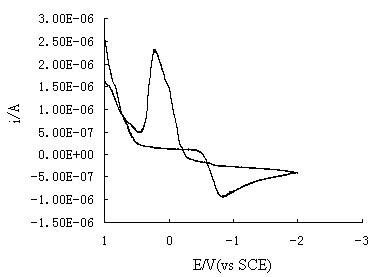
Fig.1 Cyclic voltammogram for non-etched wafer in the solution of
0.0001mol/L AgNO3+0.6mol/L NH4OH . Scan rateŁş50mV/s.
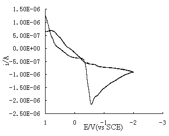
Fig. 2 Cyclic voltammogram for the etched wafer in the solution of 0.0001mol/L AgNO3+0.6mol/L NH4OH . Scan rateŁş50mV/s.
2.2 Effect of Ag+ concentration on CV behavior
ˇˇ ˇˇˇˇˇˇˇˇˇˇˇˇˇˇˇˇˇˇˇˇˇˇˇˇˇˇˇˇ
Fig. 3 shows the cyclic voltammograms of Ag(NH3)2+
ions at different concentrations. With the increase of the Ag(NH3)2+
ion concentration, whether reduction current or oxidation current linearly increases with
the concentration. At the same time, there is a shoulder-like peak occurs at more negative
potential as seen in Fig.2. It seems that the peak should be assigned to a bulk
deposition(BD) of Ag(NH3)2+ ion and the relatively
positive peak be assigned to a monolayer formation process of underpotential deposition
(UPD). However, the further experiment proved that the positive peak always increases with
the increase of Ag(NH3)2+ ion concentration in a wide
range. There is no steady peak height which corresponding to the saturated surface
coverage should be observed. So we can judge that the relatively positive peak is
not caused by 2D monolayer process of underpotential deposition and the negative one is
not the 3D process of bulk deposition. The shoulder-like peak may be caused by the surface
structure difference of the silicon substrate. Fig.4 shows the relationship between the
reduction peak current(Ipc) and square root of scanning rate(v1/2)
for using an etched silicon wafer. As it can be seen from the figure, a linear
relationship was obtained. This means that the electrode reaction is controlled by the
diffusion transition of Ag(NH3)2+ ions.
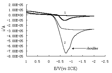
Fig. 3 Cyclic voltammograms for the etched wafer in the solutions
of (1) 0.001mol/L AgNO3+0.6mol/L NH4OH and (2) 0.01mol/L AgNO3+0.6mol/L
NH4OH . Scan rateŁş50mV/s.
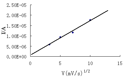
Fig. 4 The dependence between the reduction current and the root of the scanning rate. A solution of 0.01mol/L AgNO3+0.6mol/L NH4OH was used .
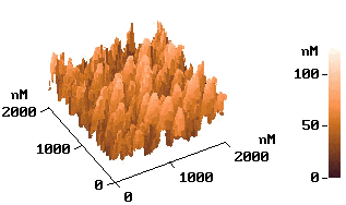
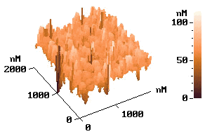
2.3 Atomic force microscopy analysis
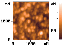
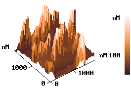
The ex situ AFM images of the wafer after electrodeposition Ag for non-etched and the
etched process were shown in Fig.5, respectively. Under the same conditions, the formed Ag
layer on non-etched wafer (a) shows island-like cluster and sparser state. The
distribution of the cluster is not even. By contrast, the surface morphology of the
deposited Ag film on the etched wafer (b) shows even island-like and intensive state.
Combining the CV results and the AFM images above, we can infer that the initial
deposition mechanism can be described by a model involving progressive nucleation on
active sites and following the hemispherical diffusion of Ag(NH3)2+
ions towards the growing 3 dimension(3D) island-like silver nucleus. These active sites on
the etched silicon substrate are much more than that of on non-etched substrate. The
nucleus size is mainly determined by the Ag-Ag interaction. Because the nucleation is
immediately followed by a 3D hemispherical diffusion of Ag(NH3)2+
ions and further by a 3D growth manner, this is the reason why no UPD was observed in the
CV experiments.
 |
 |
 a a |
 b b |
Fig.5
AFM images of the silicon surface after electrodeposition silver. (a) on non-etched wafer; (b) the etched wafer underwent a pre-electrolysis process in the solution of 0.001mol/L AgNO3 + 0.60mol/L NHOH for 40s at 1.0V.2.4 The application of electrodeposited Ag film in
electroless Ag deposition ˇˇˇˇˇˇˇˇˇˇˇˇˇˇˇˇˇˇˇˇˇˇˇˇˇˇˇˇˇˇˇˇ
Electroless method is the most frequently adopteapproach on
the ULSI metallization[1]. In this case, a catalytic seed layer is required to
initiate electroless deposition. There are two ways to get the seed layer: one is through
the electrolysis of a small amount of the metal on the wafer before electroless operation
and another one is to chemically deposit a catalytic element such as Pd and Pt on the
wafer firstly [4].
For understanding possible application of electrodeposited Ag as
a seed layer in electroless deposition of Ag, the bulk electrolysis method was employed to
prepare an Ag film. The film and a Pd seed layer were used to electrolessly deposit Ag on
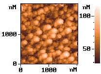
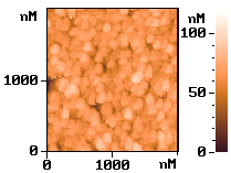
p-type silicon. Fig. 6 shows the AFM images of the electrolessly deposited silver on
silicon wafer for the different seed layers, respectively. The electrolessly deposited
silver film on the wafer of the electrolysis prepared seed layer was shown on image (a)
and the electroless deposited Ag layer on a Pd-activated wafer surface shown on image (b).
It was found that both of image a and b show similar island-like growth pattern. But the
image b with Pd-activated wafer surface has a more intensive structure.
 |
 |
 a |
 b |
Fig.6
AFM images of the silicon surface. (a) after silver electroless deposition. with electrochemical prepared seeds layer; (b) after electroless deposition silver with Pd-activated wafer.3 CONCLUSION ˇˇˇˇˇˇˇˇˇˇˇˇˇˇˇˇˇˇˇˇˇˇˇˇˇˇˇˇˇˇ
Silver was deposited on p-Si(100) wafer by using
electrodeposition method. The electrochemical behavior of electrodeposition Ag film on
silicon wafer was investigated by using CV, bulk electrolysis and AFM. The initial
deposition kinetics can be described by a model involving progressive nucleation on active
sites and following the hemispherical diffusion of Ag(NH3)2+
ion towards the growing 3 dimension(3D) island-like silver nucleus. The active sites on
etched silicon substrate are much more than that of on non-etched substrate. The nucleus
size is mainly determined by the Ag-Ag interaction. Because the nucleation is immediately
followed by a 3D hemispherical diffusion of Ag(NH3)2+ ion
and further by a 3D growth manner. Both methods of electrodeposition and electroless can
get Ag seed layer on silicon wafer. The seed layer from electrodeposition has the same
affection with a Pd-activated surface for electroless Ag deposition.
REFERENCES ˇˇ
ˇˇˇˇˇˇˇˇˇˇˇˇˇˇˇˇˇˇˇˇˇˇˇˇˇˇˇˇˇˇ
[1] Dubin V M, Shacham-Diamand Y, Zhao B et al. J.
Electrochem. Soc., 1997, 144: 898.
[2] Shacham-Diamand Y, Dubin V, Angyal M. Thin Solid Films, 1995, 93: 262.
[3] Hanbrucken M, Lay G L. Surf. Sci., 1986, 122: 168.
[4] Borensztein Y, Alameh R. Surf. Sci. lett., 1992, 274: 509.
[5] Rashkova B, Guel B, Potzschke R T et al. Electrochimica Acta, 1998, 43: 3021.
[6] Stiger R M, Gorer S, CrafB T et al. Langmuir, 1999, 15: 790.