http://http://www.chemistrymag.org//cji/2005/072019re.htm |
Feb.10, 2005 Vol.7 No.2 P.19 Copyright |
(Shanghai Institute of Microsystem and Information Technology, Chinese Academy of Sciences, 200050 Shanghai)
Abstract Quantum wells and superlattices, quantum wires, quantum dots, and complex low-dimensional structures such as QDSL-quantum dot superlattices and superlattice nanowires have been employed to increase the figure of merit (ZT) of the material, by electron band gap engineering and phonon-pocket engineering. Recent developments in low-dimensional thermoelectric materials correlative mainly with electron band gap engineering have been reviewed, including
both the theoretical basis and experimental verification. The further researches on these low-dimensional thermoelectric materials and structures should be strengthened, especially developing the new techniques of material preparation and methods of the measurements on thermoelectric properties for low-dimensional thermoelectric materials.Keywords thermoelectric materials; quantum wells and superlattices; quantum wires; quantum dots
1. INTRODUCTION
The performance of thermoelectric devices is determined by the figure of merit (ZT)
of the material, given by ZT=S2
A limit to Z is obtained in bulk materials because S, s , and kT are interdependent, and S is improvedĢŽaccompanied by s decreasing, or s is improved, accompanied by S and kT decreasing. So far, best bulk material (Bi0.5Sb0.5Te3) has ZT~1 at room temperature ( Kantzidis et al.[11] recently have shown n-type cubic bulk thermoelectric materials AgPbmSbTe2+m could be produced, which exhibited a high thermoelectric figure of merit materials ZTmax of ~2 at 800 Kelvin, with m=8 and 18 and doped appropriately). Low-dimensional quantum thermoelectric materials offer new ways comparative with bulk materials to manipulate the electron and phonon properties of a given material by electron band gap engineering and phonon engineering [1,12]. Low dimensions can give additional control. Enhanced density of states due to quantum confinement effect increases S without reducing s , and boundary scattering at interfaces reduces kT more than s . In 1993, Hicks and Dresselhaus[13] predicted that it might be possible to increase Z of thermoelectric materials, such as highly anisotropic materials, preparing them in quantum well superlattice structures. General theoretical considerations[14] suggested that, 1D quantum wires could have an even larger enhancement in ZT than 2D quantum wells due to their increased quantum confinement effect. It has also the possibility of phonon-pocket engineering to further improve ZT[12,15]. This article has reviewed the recent development in low-dimensional thermoelectric materials correlative with electron band gap engineering.
2. LOW-DIMENSIONAL THERMOELECTRIC MATERIALS
In semiconductors, electrons and holes carry charge, whereas lattice vibrations or
phonons dominate heat transport. Electrons (or holes) and phonons have two length scales
associated with their transport-wavelength,
2.1 Quantum well and superlattice thermoelectric materials
There are three generic approaches to enhance ZT of thin film thermoelectric materials including superlattice structures. One involves the use of quantum-confinement effects to obtain an enhanced density of states near the Fermi energy[13,17]: As a result, a sufficient density of charge carriers can exist in the solid to maintain the electrical conductivity, but the Fermi energy is small, and this leads to a large S. The second approach[3,18,19,20] involves phonon-blocking/electron-transmitting superlattices. The mechanism is that superlattice structures utilize the acoustic mismatch between the superlattice components to reduce kL, rather than using the conventional alloy approach, thereby potentially eliminating alloy scattering of carries. The third approach[21,22] is based on thermionic effects in heterostructures. In order to obtain high ZT of superlattice materials, it has to consider to optimize the grown directions, periodic number, and the widths of quantum-well layers, reducing the negative effect of the barrier regions and tunneling between quantum wells[23].
The first proof of principles experiment to confirm the enhancement of ZT within a quantum well was reported for n-type PbTe quantum wells within PbTe/EuxPb1ĻCxTe superlattices[24]. Soon, it was shown that an enhanced Z could also be observed for p-type PbTe quantum wells[25,26]. Herein thermoelectric devices depend on both n-type and p-type legs, the above works are rather significant for making quantum well thermoelectric devices. Harman's group[26] also demonstrated that for PbTe/Te superlattices, obtained by the addition of a few nanometers of Te above the PbTe layer before the barrier layer was added, the ZT increased from 0.37 to 0.52 at room temperature and this increase in Z T was associated with the formation of a quantum dot structure at the interface. This work induced the study on QDSLs (quantum dot superlattices).
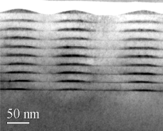 Fig.1 Ge quantum dot superlattices: 10-period Ge 1.5 nm/Si 20 nm[8]
QDSLs structures have a
delta-function distribution of density of states and discrete energy levels due to
three-dimension quantum, a potentially more favor carriers scattering mechanism, and a
much lower lattice thermal conductivity[27]. Wang et al.[8,28-31]
researched on phonons and thermal conductivities of Ge QDSLs (Fig1). They thought[6]
that multiple scattering effect/strain relaxation effect lay in Ge QDSLs, and brought
forward thermal conductivity modeling of Ge QDSLs . They introduced Raman scattering to
probe acoustic and optical phonon, and found acoustic phonons in Ge QDSLs were at the
bottom of multiple scattering effect, however, optical phonons were at the bottom of
strain relaxation effect. In 2000, Harman[32] reported ZTĄÝ2 just above room temperature for PbSeTe-based QDSLs, and in 2002,
they[27] gained PbSeTe-based QDSL thermoelectric materials by MBE (molecular
beam epitaxy) and devices with a substrate, bulk-like slab of nanostructured PbSeTe/PbTe
as n-type leg and a mental wire as the p-type leg. Device measurements indicated the
attainment of device ZdT and a material or intrinsic ZT in
the range of 1.3 to 1.6 at room temperature[27].
Bi2Te3/Sb2Te3 superlattices
are also very important low-dimension thermoelectric materials. In 2001,
Venkatasubramanian et al.[20] reported thin film thermoelectric materials
(across-plane superlattices) that demonstrated a significant enhancement , achieved by
controlling the transport of phonons and electrons in the superlattices, in ZT at
300 K. This amounted to a maximum observed factor of ~2.4 for the p-type Bi2Te3/Sb2Te3
superlattice devices by phonon-blocking/electron-transmitting (but ZT<1.4 in n-type Bi2Te3/Bi2Te2.83Se0.17
superlattices). The p-type Bi2Te3/Sb2Te3
superlattices held in highly ZT than n-type Bi2Te3/Bi2Te3-xSex
superlattices, because p-type Bi2Te3/Sb2Te3 superlattices
had "ideal" components-hand-shake of phonons
from one layer to other difficult and n-type Bi2Te3/Bi2Te3-xSex
superlattices had Ą°non-idealĄą components with perhaps some interlayer mixing-hand-shake of
phonons from one layer to other relatively easy, which made the former lattice thermal
conductivity fall to 2.5 mW/cm-K and latter lattice thermal conductivity closer to that of
bulk alloys along c-axis (5.8 mW/cm-K)[3,20].
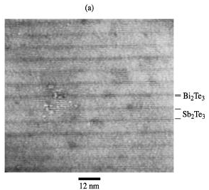
Fig.2 shows the high-quality 10?/50? Bi2Te3/Sb2Te3
superlattice structure[33]. Fig3 is the anticipated Bi2Te3/Sb2Te3
heterojunction band diagram[20]. Such ultra-short-period superlattices offer
significantly higher in-plane carriers mobility (parallel to the superlattice interfaces)
than alloys, owing to the near absence of alloy scattering and random interface carriers
scattering. Venkatasubramanian group showed that the enhanced carrier mobility in
monolayer-range superlattices was effective in the cross-plane direction for certain
superlattices, where they also obtained reduced KL and an enhanced ZT[20,33].
 |
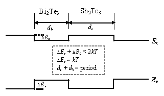 |
| Fig.2 10Å/50Å Bi2Te3/Sb2Te3 superlattice structures[33] | Fig.3 The anticipated heterojunction band diagram of Bi2Te3/Sb2Te3 superlattices[19] |
In-plane quantum wells and
cross-plane superlattices are different in the mechanism altering the transport processes
and approaches in devices[3]. In-plane quantum wells utilize quantum
confinement to get efficient heat energy transport by electrons, current and heat
transport parallel to the quantum-well interfaces. Cross-plane superlattices utilize
interfaces to impede phonons that cause undesired reverse flow of heat but not impede
forward flowing electrons, current and heat transport perpendicular to the superlattice
interfaces, and it is easy adaptability for device implementation. In approaches in
devices in-plane quantum wells need thick epi layers that need bulk-like or MEMS-like
processing, however, cross-plane superlattices need much thinner epi layers, integrated
conventional microelectronic processing.
2.2. Quantum wire thermoelectric materials
Quantum wires systems have attracted a great deal of research interest because
stronger increases in Z have been predicted[14]. The quantum confinement
of carriers in the two dimensions normal to the wire axis significantly changes their
electronic energy states, and makes the transport properties of these one-dimensional ~1D
systems very different from their bulk counterparts.
Bismuth, which is a semimetal with very small electron effective-mass
tensor components, resulting a large spatial extent of the electron wave functions that
increases the effects of quantum confinement along certain crystallographic directions in
this semimetal, a highly anisotropic Fermi surface, high mobility carriers, and the
heaviest nonradioactive element to lead a small kT, is a good candidate
to study quantum-confinement effects in a 1D system and a very promising material for
thermoelectric applications when in the semiconducting regime, under heavy doping
conditions[1,14]. Bulk Bi is a semimetal with equal concentrations of electrons
and holes, thus leading to a nearly complete cancellation between the positive and
negative contributions to the Seebeck coefficient. By introducing quantum confinement, a
semimetalĻCsemiconductor transition can be achieved
because the band edge for the lowest subband in the conduction band rises above that for
the highest subband in the valence band [1], and by adjusting the doping level
carefully, an enhancement in the thermoelectric figure of merit over its bulk form is
expected.
In particular, a semimetal-to-semiconductor transition was observed as
the wire diameter was decreased from 100 to 60 nm, and electron localization effects
became visible in wires of diameters below 50nm[6,34,35]. In 1999, Sun et al.[36]
set up a theoretical modeling of thermoelectricity in Bi nanowires to predict the relation
of thermoelectric properties and the band structures on nanowire width, found that the
optimized n-type quantum wire, the value of Z1DT was
almost 1.5 for wire diameter ~10 nm, while for the p-type quantum wire, the optimal
Z1DT was only 0.12, and predicted that values of Z1DT
above 1.0 could be achieved with wire widths smaller than 11.4 nm for n-type,
and smaller than 4.5 nm for p-type Bi nanowires, showing that thinner p-type
quantum wires were needed to get comparable Z1DT values. In 2000,
an enhancement of the figure of merit to a value of ZT ~6 (at 77 K) was predicted[37]
for wires with 5 nm diameters, doped to 1018 electrons per cm3.
Heremans and Thrush et al.[37] studied galvanomagnetic
properties, dependence of the electrical resistance, longitudinal magnetoresistance and
transverse magnetoresistance, of single-crystal bismuth nanowires arrays, with diameters
of 7 to 200 nm, embedded in an amorphous porous anodic alumina matrix. A theoretical model
for the transport properties of cylindrical Bi nanowires was also developed[38],
and the results showed the trigonal axis was the most favorable wire orientation for
thermoelectric applications, and Z1DT >1 was predicted for n-type
trigonal wires with diameters dw<10 nm. The effect of the §Ī-point holes on Z1DT was also investigated[38].
It was found that Z1DT could be significantly enhanced,
especially for p-type Bi nanowires, if the G-point holes were removed or suppressed. Heremans and Thrush[39]
reported the measurements of the thermoelectric power and longitudinal magneto-Seebeck
coefficient of 200 nm diameter single-crystal bismuth nanowires, which were metallic and
showed no enhancement in S, as expected, and pointed out, by theoretically
calculating, that bismuth nanowires should have a strongly increased thermoelectric figure
of merit over bulk Bi, when the diameter was decreased below about 10 nm. While the
theoretical basis for the increase in S and Z has been developed,
experimental verification of these effects has been difficult to realize. In 2002,
Heremans and Thrush[40] reported the first experimental observation of a very
large enhancement of the thermoelectric power of composites containing bismuth nanowires
with diameters of 9 and 15 nm, embedded in porous alumina and porous silica.
Template-assisted nanowire fabrication has been developed for growing
large-scale order arrays of Bi nanowires[1,6,40] because a single nanowire will
not transport enough current to make a workable device. The methods of filling an array of
parallel nanochannels with the media of interest include pressure injection, vapor
deposition, and electrochemical deposition. Pressure injection, technique is limited to
wires with diameters greater than 40 to 50 nm, because the necessary pressure increases
rapidly with decreasing diameter[42]. The vapor-phase technique, not relying on
pressure to insert the host material into the pores of a host material, has been applied
to prepare wires of diameters down to 7 nm[37]. Electrodeposition, easy in
making good electrical contacts, is very attractive for filling the pores of an alumina
template. The polycystic nanowire arrays, produced by electrodeposition, were expected to
have lower carrier motilities than the crystalline arrays prepared by filling from the
vapor phase or by pressure injection[1].
Sb and Bi are both group V elements, semimetal in bulk form, completely
miscible with each other, so if introduction of Sb in Bi moves down the G-point valence band edge energy
relative to the L-point edges, it will provide a promising approach to achieve
desirable band structure (i.e., semiconducting) in Bi nanowires[1]. As Bi1-xSbx,
of particular interest for thermoelectric applications is the low Sb concentration range (x<0.07)
where the bulk material is semimetallic, the regions for 0.07<x<0.09 and
0.16<x<0.22 where bulk Bi1ĻCxSbx
is an indirect gap semiconductor and finally the region 0.09<x<0.16 where
bulk Bi1-xSbx is a direct gap semiconductor (Fig.4)[1,41,42].
Fig.4 shows that the dependence of wire diameter and semimetal-semiconductor transition of
Bi1ĻCxSbx
nanowires and that how the variation of the nanowire diameter can be used to change the
electronic structure quite dramatically with no basic change occurring in the crystal
structures[6,41,42,43]. The point at x=0.13 in Bi1-xSbx,
and a wire diameter of 60nm, is very interesting, because where the L-point, G-point and H-point hole
subband edges are all degenerated with one another, leading to a very large density of
hole states to enhance Seebeck coefficient.
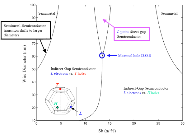
Fig.4 Phase diagram of electronic
band structures of Bi1-xSbx nanowires[6,41]
Dresselhaus group[6,43,44]
found that 65-nm Bi1-xSbx nanowires exhibited
semimetal-semiconductor transition behaviors similar to those of pure Bi nanowires, ZT
of both p-type and n-type Bi1-xSbx nanowires was
increased, and ZT performance of practical interest could be achieved at
experimentally accessible wire diameters: n-type and p-type nanowires have matched ZT
(~1.2) at a wire diameter of ~ 40 nm and Sb concentrations of x~0.13. They
investigated[6,43] the boundary and impurity scattering effect by the
measurement of magnetoresistance, and found that magnetoresistance of 65-nm Bi1-xSbx
nanowire arrays exhibited a maximum at B~4T due to the boundary scattering,
suggesting that ballistic transport phenomena be possible, and magnetoresistance of 40-nm
Bi1-xSbx wires decreased with increasing Sb
concentration x, while that of 65-nm wires increased. In 2001, Dresselhaus et al.[45]
predicted enhancements in ZT for Bi1-xSbx nanowires
with diameters of 35-50 nm, which would guide the further research on them.
It is propitious to filling the high density of pores in porous alumina
with Bi1-xSbx nanowires by electrodeposition. Gonzalez
et al.[46] obtained dense, continuous, and highly crystalline Bi0.84Sb0.16
200-nm wire arrays, using porous alumina as a template, from a nonaqueous solvent by
electrodeposition technique. However, this was independent of quantum effect. Bi2Te3
and (Bi, Sb)2Te3 polycrystalline nanowires or quantum wires were
also prepared by electrodeposition technique[47,48]. In 2003, Snyder et al.[49]
fabricated thermoelectric microdevice by a MEMS (microelectromechanical system) ĻClike electrochemical process. They prepared n-type and p-type
(Bi,Sb)2Te3 thermoelectric elements by electrodeposition, and showed
the fascination of this technology for thermoelectric microarrays.
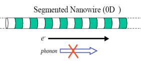
Segmented nanowires or superlattice nanowires(superlattice in a 1D
system) are also applied to increase ZT by taking advantage of both the
superlattices and the nanowires to design a better thermoelectric system, substantially
reduce the lattice thermal conductivity by increasing the phonon scattering at the segment
interfaces, and gain insight and understanding of the enhanced thermopower S (and
the power factor S2s ) in quantum dot arrays and cross-plane
superlattice systems[6,9,10,43]. Fig.5a is the schematic diagram of a
superlattice nanowire consisting of interlaced nanodots[6]. In 2002, Wu et al.[9]
synthesized single-crystalline Si/SiGe superlattice nanowires (Fig5.b), growth in a
block-by-block fashion, and with longitudinal ordered heterostructures, by hybrid pulsed
laser ablation/chemical capor deposition (PLA-CVD) process. In 2003, Lin and Dresselhaus[10]
reported a theoretical model for the electronic structure and transport properties of
superlattice nanowires, predicted that a potential barrierĻCwell inversion induced by quantum confinement, which was a unique
phenomenon in superlattice nanowires, and pointed out ZT values higher than 4 and 6
were predicted for 5-nm-diameter PbSe/PbS and PbTe/PbSe superlattice nanowires at 77 K,
respectively.
 ĄĄ
ĄĄ 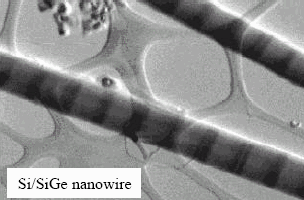
a
b
Fig.5 Segmented nanowires or superlattice nanowires
a. Schematic diagram of a superlattice nanowire consisting of interlaced nanodots [6]
b. STEM image Si/SiGe superlattice nanowires[9]
2.3 Quantum dot thermoelectric materials
Since the enhancement in thermoelectric properties was anticipated to be more
pronounced as the dimensionality decreased, 0D structures held even greater promise than
1D and 2D systems. However, unlike 1D or 2D systems, where at least one of the directions
is not quantum confined and thus can provide electrical conduction, 0D structures, such as
quantum dots, are confined in all directions, and this may present difficulties for some
applications[10].
3. CONCLUSION
Modern electronic microdevices, such as microprocessors, microsensors,
microcontrollers, and microinstruments, have significantly reduced power requirements but
at the same time require more attention in terms of integrated thermal management and
power management and distribution. Micro thermoelectric converters are considered a
promising technology approach for meeting some of these new requirements. Thus worldwide
efforts are undertaken to expand the technology for thermoelectric devices into the field
of typical microsystem technologies including aspects of low-dimensional high ZT
material[50]. Quantum wells and superlattices, quantum wires, quantum dots, and
complex low-dimensional structures such as QDSL-quantum dot superlattices and superlattice
nanowires have been found to improve obviously the performance of thermoelectric
materials, by enhanced density of states due to quantum confinement effect and boundary
scattering at interfaces. In spite of the merit in low-dimensional thermoelectric
materials, there are some new challenges in their materials synthesis and
characterization, such us the determination of the Seebeck effect can be quite tricky for
superlattices that are grown on substrates and buffers because the substrate may make a
large contribution to the overall measured properties[1]. The technique about
illumining thermal and thermoelectric characterization of nanostructures or
low-dimensional structures has to be further developed, as well as the new methods of
materials synthesis and microdevices production.
REFERENCES
[2] Kanatzidis M G, Hogan T, Mahanti S D et al. New thermoelectric materials and devices at Michigan State University, DARPA-ONR-DOE high efficiency thermoelectric workshop, in San Diego, California, March 24-27, 2002.
[3] Venkatasubramanian R. Superlattice Thermoelectric materials and devices. DARPA-ONR-DOE high efficiency thermoelectric workshop, in San Diego, California, March 24-27, 2002.
[4] Bass J C. Potential quantum well thermoelectric applications, DARPA-ONR-DOE high efficiency thermoelectric workshop, in San Diego, California, March 24-27, 2002.
[5] Virden J, Elsner N. Scale up of quantum well/superlattice thermoelectric devices, DARPA-ONR-DOE high efficiency thermoelectric workshop, in San Diego, California, March 24-27, 2002.
[6] Dresselhaus M S. Nanowires for thermoelectric applications, DARPA-ONR-DOE high efficiency thermoelectric workshop. in San Diego, California, March 24-27, 2002.
[7] Andreev A V, Matveev K A. Phys. Rev. Lett., 2001, 86 (2): 280-283.
[8] Wang K L, Liu J L, Phonons A K. Thermal conductivities of Ge quantum dot superlattices, DARPA-ONR-DOE high efficiency thermoelectric workshop, in San Diego, California, March 24-27, 2002.
[9] Wu Y Y, Fan R, Yang P D. Nano. Lett., 2002, 2 (2): 83-86.
[10] Lin Y M, Dresselhaus M S. Phys. Rev. B, 2003, 68: 075304 (1-14).
[11] Hsu K F, Loo S, Kantzidis M G et al. Science, 2004, 303: 818-820.
[12] G. Chen, T. Zeng, D. Song et al. Materials Science and Engineering: A, 2000, 292: 155ĻC161.
[13] Hicks L D, Dresselhaus M S. Phys. Rev. B, 1993, 47 (19): 12727-12731.
[14] L. D. Hicks, M. S. Dresselhaus. Phys. Rev. B, 1993, 47 (24): 16631-16634.
[15] Chen G. Characterization, devices, and modeling, DARPA-ONR-DOE high efficiency thermoelectric workshop, in San Diego, California, March 24-27, 2002.
[16] Majumdar A. Science, 2004, 303: 777-778.
[17] Harman T C, Taylor P J, Spears D L et al. IEEE In proc. 18th int. conf. on thermoelectrics (ed. Ehrlich, A.), Piscataway, NJ, 1999: 280-284.
[18] Venkatasubramanian R. Naval Res. Rev., 1996, 58: 31-40.
[19] Lee S M, Cahill D G, Venkatasubramanian R. Appl. Phys. Lett., 1997, 70: 2957-2959.
[20]Venkatasubramanian R, Siivola E, Colpitts T et al. Nature, 2001, 413: 597-602.
[21] Mahan G D, Woods L M. Phys. Rev. Lett., 1998, 80: 4016-4019.
[22] Shakouri A, Bowers J E. Appl. Phys. Lett., 1997, 71: 1234-1236.
[23] Broido D A, Reinecke T L. Appl. Phys. Lett., 1995, 67 (1): 100-102.
[24] Hicks I D, Harman T C, Dresselhaus M S et al. Phys. Rev. B, 1996, 53: 10493ĻC10496.
[25] Harman T C, Spears D I, walsh M P et al. IEEE In proc.16th int. conf. on thermoelectrics, 1997: 416ĻC423.
[26] Harman T C, Spears D I, Walsh M P. J. Electron. Mater. Lett., 1999, 28: L1ĻCL4.
[27] Harman T C, Taylor P J, Walsh M P et al. Science, 2002, 297: 2229-2232.
[28] Liu J L, Khitun A, Wang K L et al. Phys. Rev. B, 2003, 67: 165333(1-6).
[29] Khitun A, Wang K L. Appl. Phys. Lett., 2001, 79 (6):851-853.
[30] Khitun A, Balandin A, Wang K L et al. J. Appl. Phys., 2000, 88: 696-699.
[31] Liu J L, Wan J, Wang K L et al. J. Appl. Phys., 2002, 92: 6804-6808.
[32] Harman T C, Taylor P J, Spears D L et al. J. Electron. Mater. Lett., 2000, 29: L1-L4.
[33] Venkatasubramanian R, Colpitts T, Lamvik M et al. Appl. Phys. Lett., 1999, 75: 1104-1106.
[34] Zhang Z, Sun X, Dresselhaus M S et al. Appl. Phys. Lett., 1998, 73: 1589ĻC1591.
[35] Heremans J, Thrush C M, Dresselhaus M S et al. Phys. Rev. B, 1998, 58: R10091-R10095.
[36] Sun X, Zhang Z, Dresselhaus M S. Appl. Phys. Lett., 1999, 74 (26): 4005-4007.
[37] Heremans J, Thrush C M, Dresselhaus M S et al. Phys. Rev.B, 2000, 61(4): 2921-2930.
[38] Lin Y M, Sun X Z, Dresselhaus M S. Phys. Rev. B, 2000, 62 (7): 4610-4623.
[39] Heremans J P, Thrush C M. Phys. Rev. B, 1999, 59 (19): 12579-12583.
[40] Heremans J P, Thrush C M, Morelli D T et al. Phys. Rev. Lett., 2002, 88 (21): 216801(1-4).
[41] Lenoir B, Cassart M, Michenaud J P et al. J. Phys. Chem. Solids, 1996, 57: 89ĻC99.
[42] Lenoir B, Dauscher A, Cassart M et al. J. Phys. Chem. Solids, 1998, 59 (1): 129-134.
[43] Dresselhaus M S, Lin Y M, Dresselhaus G et al. Materials Science and Engineering: C, 2003, 23(1-2): 129-140.
[44] Lin Y M, Rabin O, Dresselhaus M S et al. Appl. Phys. Lett., 2002, 81:2403ĻC2405.
[45] Rabin O, Lin Y M, Dresselhaus M S. Appl. Phys. Lett., 2001,79: 81ĻC83.
[46] Gonzalez M M, Prieto A L, Knox M S et al. Chem. Mater., 2003, 15: 1676-1681.
[47] Prieto A L, Sander M S, Gonzalez M M et al. J. Am. Chem. Soc., 2001, 123: 7160-7161.
[48] Gonzalez M M, Prieto A L, Gronsky R et al. Adv. Mater., 2003, 15 (12): 1003-1006.
[49] Snyder G J, Lim J R, Huang C K et al. Nature Mater., 2003, 2: 528-531.
[50] Bottner H. IEEE In proc. 21th int. conf. on thermoelectrics, 2002: 511-518. ĩÍÎŽČČĩįēÄÁÏŨîÐÂ―øÕđ
đØÓÂŧÔĢŽ―âū§ÓĻ
ĢĻÖÐđúŋÆŅ§ÔšÉÏšĢÎĒÏĩÍģÓëÐÅÏĒžžĘõŅÐūŋËųĢŽÉÏšĢ 200050ĢĐ
ÕŠŌŠ ÁŋŨÓÚåÓëģŽū§ļņĄĒÁŋŨÓÏߥĒÁŋŨÓĩãŌÔž°ļīšÏĩÍÎŽ―áđđĢŽČįĢšÁŋŨÓĩãģŽū§ļņšÍģŽū§ļņÄÉÃŨÏßĢŽķžÄÜÍĻđýĩįŨÓÄÜīøđĪģĖšÍÉųŨÓđĪģĖĖáļßēÄÁÏĩÄÓÅÖĩ(ZT )ĄĢīÓĀíÂÛšÍĘĩŅéÁ―·―ÃæŨÛĘöÁËĩÍÎŽČČĩįēÄÁÏÓëĩįŨÓÄÜīøđĪģĖÏāđØĩÄŨîÐÂ―øÕđĄĢĩÍÎŽČČĩįēÄÁÏž°―áđđÐč―øŌŧē―ŅÐūŋĢŽÓČÆäĘĮ·ĒÕđÆäÖÆąļ·―·Ļž°ÆäČČĩįÐÔÄÜēâÁŋ·―·ĻĄĢ
đØžüīĘ ČČĩįēÄÁÏ; ÁŋŨÓÚåšÍģŽū§ļņ; ÁŋŨÓÏß; ÁŋŨÓĩã